PCB Lab Manufacturer,Supplier and Exporter in India
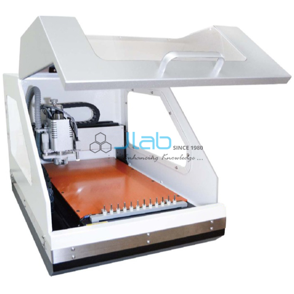
Product Code : JL-PFS-10406
Jlab Export is a leading PCB Lab Manufacturer,and suppliers in India, PCB Lab Manufacturer,and suppliers in South Africa, PCB Lab Algeria (Algiers), PCB Lab Angola (Luanda), PCB Lab Argentina (Buenos Aires), PCB Lab Armenia (Yerevan), PCB Lab Australia (Canberra), PCB Lab Austria (Vienna), Bahrain (Manama), Bangladesh (Dhaka), Bhutan (Thimphu), Bolivia (Sucre), Botswana (Gaborone), Brazil (Brasília), Brunei (Bandar Seri Begawan), Montenegro (Podgorica), Morocco (Rabat), Mozambique (Maputo), Myanmar (Naypyidaw), Namibia (Windhoek), Nepal (Kathmandu), New Zealand (Wellington), Nigeria (Abuja), Oman (Muscat), Palestine (Ramallah), Panama (Panama City), Papua New Guinea (Port Moresby), Paraguay (Asunción), Peru (Lima), Philippines (Manila)¸ Portugal (Lisbon), Qatar (Doha), Rwanda (Kigali), Saudi Arabia (Riyadh), Senegal (Dakar), Serbia (Belgrade), Sierra Leone (Freetown), Slovakia (Bratislava), South Africa (Cape Town) (Pretoria) (Bloemfontein), South Sudan (Juba), Spain (Madrid), Sri Lanka (Sri Jayawardenepura Kotte) (Colombo), Sudan (Khartoum), Syria (Damascus), Tanzania (Dodoma), Thailand (Bangkok), Togo (Lomé), Tonga (Nuku'alofa), Trinidad and Tobago (Port of Spain), Tunisia (Tunis), Turkey (Ankara), Turkmenistan (Ashgabat), Uganda (Kampala), United Arab Emirates (Abu Dhabi), United Kingdom (London), United States (Washington, D.C.).